
Company Profile
Nano Electronics and Micro System Technologies, Inc. (hereinafter referred to as “NEMS”) was established in June 2002, and is a professional plasma equipment development and manufacturing company in Taiwan. The company focuses on the core businesses of plasma cleaning, plasma etching, and plasma surface modification technology, and has constructed a complete plasma technology platform covering the three major systems of vacuum plasma, atmospheric pressure plasma, and high-efficiency plasma torch that are widely used in processes such as surface cleaning, etching, desmearing, poling, coating pretreatment, and high-temperature decomposition. Unlike traditional equipment manufacturers, NEMS has precise control capabilities for multiple parameters, such as gas composition, chamber pressure, energy density, and material thermal shock. It can flexibly respond to 3D structural and high aspect ratio process challenges, demonstrating its adaptability in highly modular and cross-domain applications.
Main Competitive Advantages
Technological Innovation and Process Integration Capabilities
NEMS has long been dedicated to the field of plasma technology, focusing on the niche market of plasma surface treatment. With a self-developed high-density plasma source design and cross-material integration capabilities (covering ABF, glass, silicon, and silicon carbide), combined with its AI process optimization platform and intelligent operation system, the company has created an operational model of “process as a service.” NEMS also has a professional plasma technology team and multiple patents, demonstrating high flexibility in customization and process integration capabilities. With the advantage of rapid response and innovative R&D, NEMS can provide exclusive module design, process parameter optimization, and material testing services according to customer needs to effectively shorten development time and improve process yield.
Diversified Product Layout and Cross-industry Applications
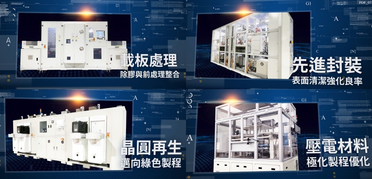
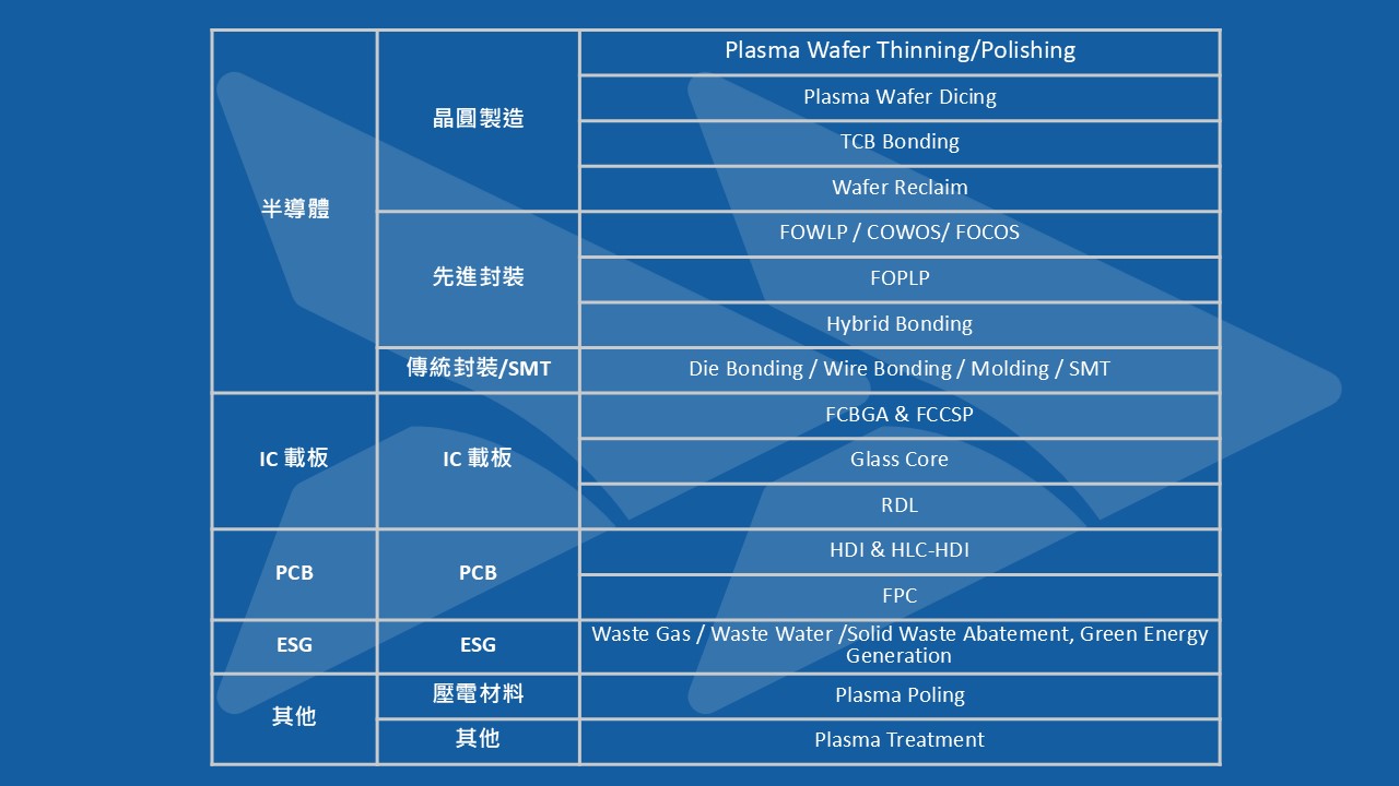
NEMS’s product line spans semiconductor plasma poling and etching equipment, IC substrates, and PCB process-specific machines. It also extends to new energy and environmental protection application equipment, including green technology fields such as plasma exhaust gas and wastewater treatment systems, methane decomposition hydrogen production equipment, and high-temperature volume reduction systems. NEMS also has the ability to develop both vacuum plasma and atmospheric plasma equipment, integrating and applying cross-industry technologies deeply, and can flexibly meet the needs of diverse manufacturing processes.
Advanced Packaging and Leading Heterogeneous Material Manufacturing Process
With the rapid evolution of 2.5D/3D packaging and hybrid bonding technology driven by AI and high-performance computing (HPC), NEMS is actively entering the advanced packaging market and investing in heterogeneous material etching and surface activation technology to provide integration solutions for packaging processes involving Epoxy+SiO₂, Glass+Cu, and others. NEMS has received verification from leading wafer reclaim companies, and its back-end desmearing and polymer removal equipment has also been steadily mass-produced, establishing a leading position in advanced packaging and heterogeneous integration processes.
Industry Status and Market Prospects
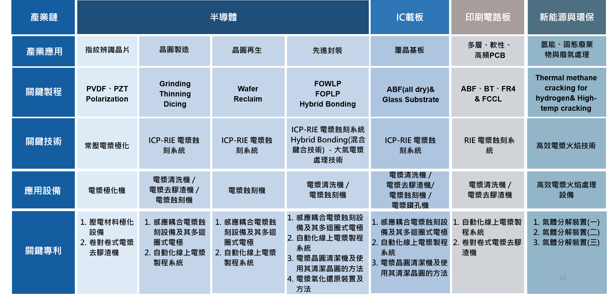
NEMS focuses on plasma process technology and has established a diversified layout in the upstream, midstream, and downstream sectors of the semiconductor, IC substrate, and PCB industries. The products encompass a complete process chain, including front-end etching, middle-end substrate treatment, back-end desmearing, and waste gas treatment, thus forming a unique technological integration advantage. As the global semiconductor industry enters the era of advanced packaging and new material applications, the demand for plasma equipment continues to grow. Driven by ESG trends and the net-zero emission policy, plasma technology, with its low pollution, high efficiency, and energy-saving characteristics, is further expanding its application scope to green energy and reclaimator process. NEMS is expected to become a representative enterprise in Taiwan’s plasma technology and equipment industry, playing a key role in the global supply chain.
Future Prospects
Looking ahead to the future, NEMS will use “technological innovation” and “in-depth market cultivation” as dual growth engines to continuously strengthen its smart manufacturing and AI process control capabilities while deepening strategic cooperation with international giants to expand its market presence in Europe, America, and Asia. At the same time, NEMS will actively develop applications in the fields of environmental protection and new energy, and implement ESG practices and green supply chain integration in order to move toward the goal of becoming a leading plasma equipment solution supplier in the Asia-Pacific region.